World Wide Suppliers of Industrial Sapphire&Ruby Precision Parts
Sapphire to Metal for Fluidic,Metrology&Medical Components
ISO 9001:2019 Mfg&Managment Certified Companies
-
- Sapphire Lens
- IPL Light Guides
- Sapphire Prism
- Zirconia Ceramic Parts
- Single Crystal Silicon Carbide(SiC 6H/ 4H)
- Optical Windows
- Optical Lens
- Sapphire Substrate&Wafer
- CMM Styli - Probe Tips
- Sapphire Orifice Jewel
- Sapphire Windows
- Jewel Bearing
- Sapphire Tube&Rods
- Balls&Semisphere
- Ruby Orifice Nozzle
- Sapphire&Ruby Assembly Parts
- Sapphire&Ruby Nozzle
- Custom Shaped Sapphire Parts
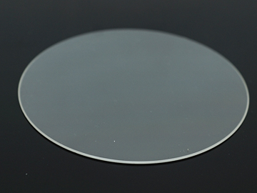
Sapphire Substrate&Wafer
Sapphire substrates are ideal for use instead of glass substrates when optical transmission is required in the ultraviolet (above 200 nm) or infrared (below 5 μm) range. Low-temperature optical measurements will also benefit from the higher thermal conductivity of sapphire substrates, and they may also be used in high temperature environments up to 2300 K.
Application
-
Microelectronic IC applications
-
SOS Silicon-on-Sapphire
-
The growth of superconducting compounds / Gallium Nitride
-
Infrared detectors
-
Hybrid microelectronics
-
Polishing carriers
-
Hostile environment
-
Optical transmission from ultraviolet to near infrared
-
High temperature
-
Radiation resistance
Specification
- Material: Sapphire Substrate
- Orientation:C-AXIS
- Thickness:0.5mm(other Thickness Ok)
- Surface:DSP
- TTV<10um
- BOW:<10um
- Warp:<10um
- Package:100 Grade Cleaning Room By Vacuum Package
- Customize:Acceptable
- Thickness Tolerannce:±15um
- Shape:Round Shape
Standard Diameter
-
2 inch C-plane sapphire wafer SSP/DSP
-
3 inch C-plane sapphire wafer SSP/DSP
-
4 inch C-plane sapphire wafer SSP/DSP
-
6 inch C-plane sapphire wafer SSP/DSP
Orientation
-
A-plane (1120) sapphire wafer
-
R-plane (1102) sapphire wafer
-
M-plane (1010) sapphire wafer
-
C-axis with a 0.5°~ 10° offcut, toward A-axis or M-axis
-
Other customized orientation
Custom Size
-
10x10x0.5mm sapphire wafer
-
20x20x0.5mm sapphire wafer
-
Ultra thin (100um) 2inch sapphire wafer
-
8 inch sapphire wafer
SSP C-plane 1.0mm/1.3mmm
DSP-C-plane 0.65mm/ 0.8mm/1.0mmt
|
6inch |
|
|
2inch |
DSP C-AXIS 0.1mm/ 0.175mm/0.2mm/0.3mm/0.4mm/0.5mm/1.0mmt |
|
3inch |
DSP/ SSP C-axis 0.43mm/0.5mm |
|
4Inch |
dsp c-axis 0.4mm/ 0.5mm/1.0mm |


 1803,2006,Huachuang Building
 0086 18623135040
 13500373464